Hardware About The MicroSD Card Connector

DayVeeBoi

Well-Known Member
Member
Joined
Aug 17, 2015
Messages
528
Trophies
0
Location
Canada
XP
968
Country
Canada
Good idea. But it will take until the sun expands for it to get here.

Also, chances are they send the wrong bit. They don't have many schematics on their listings

I agree, there are many sellers on AliExpress and other than knowing someone or having a particular supplier that you deal with it is likely that it could be a headache.
There is a supplier that I buy console parts from that actually repairs/refurbishes/salvages consoles they are unlikely to send the wrong part if you send a photo and description of what you're looking for.

As far as shipping, I use e-packet for most things, but if I broke my Switch and needed a part asap I wouldn't feel bad about spending $25 on DHL to get it within a day or two. Realistically to get it fixed outside of warranty would be much more painful.
 

Maldimer

New Member
Newbie
Joined
Nov 1, 2019
Messages
2
Trophies
0
Age
25
XP
43
Country
Italy
I never did find the correct part. It isn`t a molex.

The thinnest BTB stacking connector they do is too wide (the central raised nipple bit)

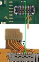
So I chopped the ribbon just in front of the smoothing cap on the SD reader and used some AWG40 to go directly to the testpads, keeping the motherboard side intact. Can post a pinout if it would help...

View attachment 149584

Hey everybody, sorry for resuming an old thread, but I came across the same problem described and I found your solution which gave me hope.
Now, since I have no competence in soldering, I wanted to take my switch somewhere and explain this solution to someone who could handle it (like a cellphone repair shop), but it isn't clear to me what you meant for "chopping the ribbon in front of the smoothing cap" (no elettronic competence and not being english can harm my understanding skills haha).
Did you mean that you cut off the male connector's wire that is used to connect the SD card reader to the female port on the motherboard?

Also, does the red link mean that the capacitor has to be soldered to that pin?

Thanks in advance :)
 
Last edited by Maldimer,

mattytrog

You don`t want to listen to anything I say.
Member
Joined
Apr 27, 2018
Messages
3,708
Trophies
0
Age
48
XP
4,328
Country
United Kingdom
Hey everybody, sorry for resuming an old thread, but I came across the same problem described and I found your solution which gave me hope.
Now, since I have no competence in soldering, I wanted to take my switch somewhere and explain this solution to someone who could handle it (like a cellphone repair shop), but it isn't clear to me what you meant for "chopping the ribbon in front of the smoothing cap" (no elettronic competence and not being english can harm my understanding skills haha).
Did you mean that you cut off the male connector's wire that is used to connect the SD card reader to the female port on the motherboard?

Also, does the red link mean that the capacitor has to be soldered to that pin?

Thanks in advance :)
The simplest way of thinking about it, is that the capacitor needs to be between the red and green trace. However you do it.

Connect the green trace, then piggyback the cap on to the green trace somewhere, and the other end is the red trace. Solder to SD reader side of the red trace.
 

Maldimer

New Member
Newbie
Joined
Nov 1, 2019
Messages
2
Trophies
0
Age
25
XP
43
Country
Italy
The simplest way of thinking about it, is that the capacitor needs to be between the red and green trace. However you do it.

Connect the green trace, then piggyback the cap on to the green trace somewhere, and the other end is the red trace. Solder to SD reader side of the red trace.

Thanks for answering, I'm really sorry for bothering you :(
So, from what I'm understanding, this is the wiring I have to do for the capacitor, right?
The green trace just goes from that thing from the motherboard to that pin on SD reader, and the capacitor is connected to that other pin through the red trace, am I right? :wacko:
I pointed out the capacitor to make sure that's the thing we're talking about.
Thanks again and sorry for being so noobish haha

mobo.jpg
 
Last edited by Maldimer,
  • Like
Reactions: manchesterraver

Matius

Well-Known Member
Newcomer
Joined
Dec 9, 2019
Messages
49
Trophies
0
Age
28
XP
185
Country
Australia
View attachment 192929


@Matius - the damaged points you mentioned go here on the flip side.

Thanks for the reply Matty.

The image I sent via PM, not sure whether it was detailed enough for the actual extensive damage, here's a much better closeup with a Microscope I managed to use.


From bottom to top:

1: Test point seems fine, actual pad for the B2B connector pad appears ripped
2: Test point appears ripped, actual pad for the B2B connector pad appears ripped
3: Test point appears fine, actual pad for the B2B connector pad appears ripped
4: Test point appears ripped, actual pad for the B2B connector pad appears ripped
5: Test point appears ripped, actual pad for the B2B connector pad appears fine
6: Test point appears fine, actual pad for the B2B connector pad appears ripped
7: Test point appears fine, actual pad for the B2B connector pad appears ripped

I really do have a hit and miss with these and it does look some some of the copper trace appears to be damaged from places. I was looking for something exactly as what you mentioned, do you happen to know where the other 5 would go to as I was hoping they would just align with the image you've posted, but it appears not. Thanks for your investigation in the matter.
 

mattytrog

You don`t want to listen to anything I say.
Member
Joined
Apr 27, 2018
Messages
3,708
Trophies
0
Age
48
XP
4,328
Country
United Kingdom
That's not too bad. I've seen worse boards.

Yeah will put rest of points up tomorrow.

As long as the board is otherwise working, that is straightforward. Only one trace needs a pigtail running round the back. The rest of them, you will get away with
 
  • Like
Reactions: Matius

Matius

Well-Known Member
Newcomer
Joined
Dec 9, 2019
Messages
49
Trophies
0
Age
28
XP
185
Country
Australia
That's not too bad. I've seen worse boards.

Yeah will put rest of points up tomorrow.

As long as the board is otherwise working, that is straightforward. Only one trace needs a pigtail running round the back. The rest of them, you will get away with

I may have misunderstood, are those two columns ( of test point pairs ) connected to each other. For example, can I use either of the points on the left or right (LIke seen in the image below). The yellow line on your diagram, the pad to the right is completely gone, so am I correct to be able to use the one to left? I wondering if they're both connected. Otherwise, I would then need to run 3 wires from the back them. I posted a diagram if it helps to show which are gone and are there.

Green = Available
Red = Gone


--------------------- MERGED ---------------------------

Connected as in the same trace I should have mentioned
 

tomsek68

Well-Known Member
Newcomer
Joined
May 19, 2018
Messages
46
Trophies
0
Age
22
XP
233
Country
Hungary
Follow the traces on the board/fpc. I cant make a diagram, as i am posting from my phone.

Also you can use pins from another connector, if you know what you are doing. I found that an iPhone screen female connector's pins will fit nice. I used one from a 5s. Desolder the connector with hot air (or tear it off the ribbon) and break the connector in half. This way two pins should fall off.
Pros:
  • No need to replace the whole connector
  • No wires to break when you start to fix the other issues on the board
  • Eliminates the danger of soldering to the wrong breakout pin
Cons:
  • It is hard to put the new pin in place (as it is so tiny)
  • You can destroy your connector even further if not careful
 
Last edited by tomsek68,
  • Like
Reactions: manchesterraver

manchesterraver

Active Member
Newcomer
Joined
Mar 3, 2020
Messages
39
Trophies
0
Age
35
XP
100
Country
United Kingdom
I had the same issue with my first switch. but I ended up using it for soldering practice to hard mod my other switches. I have just joined GBA temp but I have kept my eye on this thread for pretty much 3 months :D:D:D sacked it off in the end, because I ripped the pads off, and dont know how to fix it. but I guess I could have a go at soldering to the alt points on the other side of the board. pretty informative post.
 

Sushi4life

Active Member
Newcomer
Joined
Feb 20, 2020
Messages
26
Trophies
0
Age
43
XP
94
Country
Canada
View attachment 192929


@Matius - the damaged points you mentioned go here on the flip side.

Hello mattytrog :),

Can you please help me pinpoint the alternate points at the back to the ones on the front? My nintendo switch has a broken point colored black front your image.

Thank you in advance!
 
Last edited by Sushi4life,
  • Like
Reactions: mitcha

newgen2005

Well-Known Member
Newcomer
Joined
Dec 6, 2015
Messages
87
Trophies
0
Age
46
XP
415
Country
Can anyone advise me which wires I will need to solder?

fCGRbjy.jpg


I am assuming looking at the images below I will be working with the pink and yellow lines, just 2 wires need to be used to make contact for missing pins?

sd_connection-jpg.191749
 
Last edited by newgen2005,

thebarraster

Member
Newcomer
Joined
Mar 15, 2017
Messages
11
Trophies
0
Age
43
XP
69
Country
United States
I'm missing that pin. From the looks of the pin out it's a ground pin? If so do I just need to connect a wire to the ground on the card reader to a screw on the mobo?
 

Attachments

  • IMG_20200603_170536.jpg
    IMG_20200603_170536.jpg
    49.9 KB · Views: 284

Site & Scene News

Popular threads in this forum

General chit-chat
Help Users
  • No one is chatting at the moment.
    K3Nv2 @ K3Nv2: Lol rappers still promoting crypto